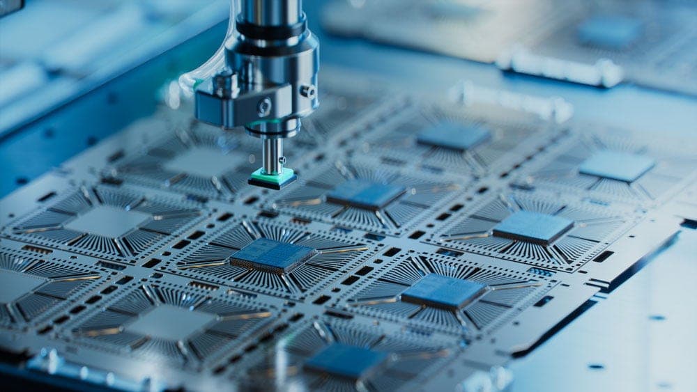
Inside the cleanrooms rising across Gujarat’s Dholera and Sanand industrial corridors, and throughout the electronics manufacturing corridors of Tamil Nadu, the visible narrative of India’s semiconductor ambition is largely one of steel, cleanroom filtration units, and automated pick-and-place equipment. Billions of dollars in capital expenditure, subsidised aggressively under the modified Semicon India Programme, have been poured into establishing outsourced semiconductor assembly and test (OSAT) and advanced packaging units. Yet, on the shop floors where initial pilot runs and high-density substrates are being routed, an uncomfortable engineering reality is setting in: laying down billions for assembly lines does not guarantee commercially viable yields.
Packaging is no longer the utilitarian back-end process of clipping lead frames and dispensing black epoxy resin. As Moor’s Law slows down at the physical silicon limit, system performance is dictated by heterogeneous integration—stacking multi-die chiplets via micro-bumps, hybrid bonding, and high-density silicon interposers. In this structural paradigm, a sub-micron defect hidden beneath five stacked dies can invalidate an entire multi-hundred-dollar module. Without native, Tier-1 capabilities in advanced metrology and physical failure analysis, Indian packaging plants face the existential threat of becoming cost-inefficient assembly houses that discard profitable silicon simply because they cannot diagnose why it failed.
The Yield Wall: Advanced Packaging as a Zero-Defect Trap
Traditional surface-mount assembly and legacy wire-bonding packaging tolerated a reasonable margin of error. If a wire bond broke or a solder joint bridged, acoustic microscopy or basic benchtop optical inspection caught the failure within minutes. But modern semiconductor packaging—encompassing 2.5D/3D architectures, fan-out wafer-level packaging (FOWLP), and high-density ball grid arrays (BGAs)—operates at tolerances that mirror front-end wafer fabrication.
When stacking chiplets, manufacturers contend with interconnect pitches dropping below 20 micrometres, with micro-bumps shrinking to sizes where even minuscule thermal expansion mismatches induce mechanical shear. The physical stress within these ultra-thin substrates creates localized warpage, non-wet micro-voids, and micro-cracking that are entirely invisible to conventional optical inspection.
If an Indian OSAT facility operates without immediate, in-line volumetric inspection capabilities, it falls into the zero-defect yield trap. In advanced heterogeneous packaging, your final yield is the cumulative product of the individual die yields and every single packaging step. If a firm packages six known good dies onto a single substrate, and its packaging defect rate is even three percent per interconnect layer, the blended operational scrap rate escalates exponentially. The cost is not merely the lost substrate; it is the destruction of six expensive, fully functional silicon dies imported from external foundries.
Without internalised, real-time metrology, an assembly plant is operating blind. The financial delta between a thriving packaging giant and an operation burning through state subsidies lies entirely in the speed at which it identifies, isolates, and rectifies yield degradation on the production line.
The Instrumentation Deficit: Beyond Simple Optical Tools
To inspect the interior of a 2.5D module, engineers cannot rely on legacy cross-sectioning and polishing, which destroys the very evidence required to diagnose a yield crash. The modern failure analysis suite requires non-destructive, sub-nanometre analytical instrumentation: high-resolution 3D X-ray computed tomography, scanning acoustic microscopy with high-frequency transducers, dual-beam focused ion beam (FIB) systems coupled with high-resolution scanning electron microscopy (SEM), and transmission electron microscopy (TEM) capable of atomic-level chemical mapping via energy-dispersive X-ray spectroscopy.
Today, India faces a severe instrumentation asymmetry. While global leaders like TSMC, ASE Group, and Amkor maintain captive, multi-million-dollar failure analysis labs within meters of their primary packaging lines, Indian packaging initiatives remain largely dependent on external, centralised academic hubs or offshore analysis centers. Sending an unverified failure sample to an analytical lab in Singapore, Taiwan, or an academic cleanroom in Bengaluru creates diagnostic latencies that span days or weeks.
In high-volume manufacturing, a two-week diagnostic cycle is an eternity. If an automated thermo-compression bonder drifts out of calibration by a fraction of a degree or applies three microns of asymmetric pressure, it will turn out thousands of defective modules before an offshore laboratory returns the cross-sectional TEM analysis identifying intermetallic compound embrittlement. Real-time yield optimization requires high-throughput in-line metrology embedded directly into the production line—tools that can measure sub-surface stress, substrate coplanarity, and void ratios at production line speed, feeding automated process control engines without interrupting cycle times.
The Talent Bottleneck: The Scarcity of Defect Pathologists
Equipment, however, is merely capital expenditure; the deeper structural choke point in India’s semiconductor ecosystem is the acute shortage of physical failure analysis specialists. Interpreting the output of a high-resolution X-ray or a lock-in thermography scan is not a routine technician job. It requires an advanced, interdisciplinary understanding of solid-state physics, physical metallurgy, polymer chemistry, and mechanical stress dynamics.
When an advanced package exhibits an intermittent electrical short at elevated operating temperatures, the underlying cause could be electromigration across a copper pillar, dielectric breakdown of an ultra-thin underfill material, or warpage-induced delamination caused by mismatched coefficients of thermal expansion. Isolating which of these phenomena occurred requires a diagnostic engineer who can perform subtle electrical fault isolation—using tools like photon emission microscopy or laser-assisted device alteration—and then direct a nanometre-precision FIB cut directly through the defect site without introducing secondary artifacts.
India’s engineering education infrastructure has historically produced exceptional digital design talent, verification engineers, and software architects. However, it has severely under-invested in specialized physical materials science and analytical instrumentation training tailored to microelectronics. While the nation’s universities graduate hundreds of thousands of engineers annually, only a tiny fraction have ever laid hands on an operational transmission electron microscope or formulated an analytical hypothesis regarding intermetallic phase transitions in lead-free solder alloys. This human capital gap leaves domestic packaging ventures heavily reliant on a small cohort of global expats or senior domestic researchers, making scale exceptionally fragile.
Geopolitical Realities: The Unspoken Tool Supply Chain
While public geopolitical discourse around semiconductors focuses almost exclusively on photolithography systems—most notably extreme ultraviolet scanners—the global supply chain for advanced metrology and failure analysis instrumentation is equally concentrated and subject to tight supply dynamics. A handful of American, European, and Japanese vendors control the market for the critical tools required to certify advanced packaging lines.
Companies such as KLA, Applied Materials, Bruker, Thermo Fisher Scientific, and Carl Zeiss produce the foundational metrology platforms, high-brightness X-ray sources, and electron-beam inspection engines that make packaging diagnosis possible. These tools carry lead times that frequently extend past twelve to eighteen months, dictated by precision optical manufacturing and complex detector supply chains.
For Indian OSAT and packaging players attempting to scale rapidly, securing priority delivery of these high-end analytical suites is a formidable challenge. Global chip foundries and incumbent packaging titans command the bulk of vendor manufacturing capacity. If an Indian packaging line is established without simultaneous priority allocation for comprehensive failure analysis tooling, it risks remaining permanently confined to mature, low-margin packaging: simple discrete packages, basic quad-flat no-leads formats, and basic legacy modules. These commoditized formats will not generate the technological learning curve or the defensible margins necessary to establish India as a genuine global hardware alternative.
Constructing the Diagnostic Substrate: The Path to Parity
Resolving this diagnostic gap requires an immediate strategic pivot from both industrial consortiums and policymakers steering the India Semiconductor Mission. Subsidising automated pick-and-place tools and cleanroom square footage is a baseline necessity, but it is insufficient to guarantee competitive survival. The operational focus must shift toward three deliberate initiatives:
First, policy mechanisms must incentivize the creation of shared, high-throughput failure analysis mega-labs situated directly within the emerging semiconductor hubs of Sanand, Dholera, and the southern manufacturing corridors. Rather than forcing every mid-tier packaging entrant or domestic component supplier to unilaterally absorb the tens of millions of dollars required for an exhaustive TEM/FIB/CT suite, sovereign-backed analytical hubs—operated under rigorous non-disclosure and commercial SLA frameworks—can provide four-hour turnaround diagnostic support to surrounding factories.
Second, the operational links between specialized research institutions—such as the Centre for Nano Science and Engineering at the Indian Institute of Science—and commercial packaging operations must be restructured. Academic cleanrooms holding advanced characterization tools must be integrated into industrial feedback loops, moving beyond basic academic inquiry into commercial yield diagnostics, while simultaneously instituting specialized failure-analysis engineering apprenticeships focused on advanced physical defect localization.
Finally, domestic equipment innovation must be deliberately nurtured around packaging-tier metrology. While developing an indigenous extreme ultraviolet scanner is an unrealistic near-term ambition, developing proprietary optical inspection engines, specialized acoustic microscopy software, automated optical defect classification models, and advanced test fixtures is entirely within the capability of India’s deep-tech hardware startups and established software ecosystem.
The coming phase of India’s semiconductor evolution will not be judged by the square footage of cleanrooms constructed or the initial ribbon-cutting ceremonies at packaging parks. The true metric of success will be measured at the edge of the silicon interposer: the speed at which Indian facilities can drive package yields from an experimental seventy percent to a commercially lethal ninety-nine percent. In that invisible, nanometre-scale battleground, advanced metrology and physical failure analysis will determine whether India’s packaging revolution becomes an enduring global pillar or an expensive assembly exercise.